Views: 0 Author: Site Editor Publish Time: 2026-07-31 Origin: Site
Final stamped part quality relies heavily on raw material precision. Dimensional variations in raw material dictate geometric dimensioning and tolerancing (GD&T) outcomes. Unpredictable inlay width variations cause missed contact zones. They increase scrap rates and lead to premature electrical failure. True position errors in stamped electrical contacts pose severe operational risks. You must tightly control material specifications and evaluate supplier capabilities when sourcing Clad Metals. Aligning material tolerances with stamping die design creates a robust technical framework. This alignment ensures the precious metal lands exactly where required on the mating surface, preventing costly downtime and compromised high-volume manufacturing yields.
Tolerance Stack-Up is Inevitable: Inlay width tolerance directly contributes to the overall tolerance stack-up, shifting the true position of the precious metal contact zone relative to the stamped part's datum reference frame.
Control of Location and Orientation: True position tolerances do not merely govern 2D location; they control both the location and orientation of the clad metal feature, preventing angular drift along the stamping path.
Referencing Strategy Dictates Yield: Designing stamping dies that reference the centerline of the inlay rather than the strip edge mitigates the impact of width variations on final contact position.
Material Selection Influences Manufacturability: The choice between an inlay clad metal strip, onlay clad metal strip, or overlay clad metal strip fundamentally alters the required stamping approach and acceptable tolerance thresholds.
Supplier Process Control is a Decision Criterion: Evaluating a clad metal supplier requires auditing their rolling, slitting, and bonding process controls, as these dictate the baseline width tolerance capability.
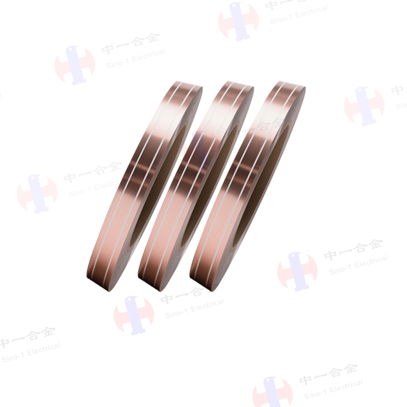
Different profiles serve distinct engineering functions on the stamping floor. An inlay clad metal strip sits flush inside the base metal. Engineers use it for smooth continuous feeding through progressive dies. The flush surface prevents snagging on guide rails. An onlay clad metal strip sits raised above the base surface. It provides a defined contact point for microswitches and relays. An overlay clad metal strip covers the entire surface. This profile suits environments demanding maximum corrosion resistance across the entire terminal.
Bonding and rolling processes inherently introduce micro-variations. Heavy reduction passes alter width and thickness slightly. The pressure required to achieve a solid state bond displaces material laterally. These microscopic shifts compound during high-speed stamping. You must account for these variations during die design. If the raw material fluctuates by a few thousandths of an inch, the die must absorb that variation without jamming or shearing the precious metal.
Clad Profile | Structural Characteristic | Stamping Die Impact | Typical Application |
|---|---|---|---|
Inlay | Flush with base metal | Allows tight guide clearances | Automotive terminals, connectors |
Onlay | Raised above base metal | Requires relieved guide rails | Microswitches, relays |
Overlay | Full surface coverage | Standard flat stock feeding | Thermostats, corrosive environments |
True position defines the exact functional contact area. ASME Y14.5 outlines how to apply this concept to stamped features. The precious metal must land exactly on the mating surface. Operational conditions demand strict control of location. You must also control orientation relative to datum features. Position tolerances prevent twist, tilt, and parallelism errors. They keep the contact face aligned down the length of the strip. If the contact face tilts by even one degree, the electrical resistance spikes.
The inlay acts as a feature of size. Applying Maximum Material Condition (MMC) modifiers allows for bonus tolerance calculations. Least Material Condition (LMC) modifiers offer similar flexibility. These modifiers balance functional requirements against manufacturing yield. When the inlay width is at its smallest acceptable size (LMC), the die has more room to position the feature without violating the outer boundary. Stamping engineers use this bonus tolerance to extend tool life between sharpenings.
Tolerance stack-up ruins perfectly designed stamping operations. Raw material inlay width tolerance adds to the base strip slitting tolerance. The positional tolerance of the stamping die adds another variable. A seemingly acceptable +/- 0.005 inch width variance causes major issues. It pushes a micro-contact entirely out of its allowable true position zone. You must map the mathematical relationship between these variables. Calculate the worst-case scenario before cutting steel for the die.
Identify the base metal slitting tolerance from the supplier specification sheet.
Add the inlay width tolerance to determine the maximum possible lateral shift.
Factor in the clearance between the strip edge and the die guide rails.
Calculate the positional tolerance of the piercing station that establishes the pilot holes.
Sum these values to find the worst-case true position deviation at the final forming station.
If the sum exceeds the allowable true position zone on the print, the part will fail inspection. You must either tighten the raw material specifications or redesign the die to reference the material differently.
Excessive inlay width variations cause physical interference. Parts fail to fit inside plastic connector housings. They jam inside mating slots. Side-to-side clearance issues destroy assembly yields. Width drift also compromises critical electrical isolation boundaries. Minimum air gaps shrink below acceptable limits. Trace and pad clearances disappear. You must translate electrical clearance concepts directly to the stamping world.
Maintain strict width controls to prevent arcing and short circuits. High-voltage applications require guaranteed minimum distances between conductive paths. If the inlay wanders too close to the edge of the terminal, the dielectric withstand voltage drops. This leads to catastrophic failure in the field. Stamping dies cannot correct raw material that is fundamentally too wide or positioned incorrectly on the base strip.
Variations in inlay width affect material feeding. The progressive stamping die relies on consistent material dimensions. Tooling clearances must accommodate the maximum material condition (MMC) of the inlay width. This necessity introduces a serious risk. The material experiences "wandering" or drift during progression. Loose guides allow the strip to shift laterally. This lateral shift destroys true position accuracy at the final forming station.
When the material is at its minimum width, the gap between the strip edge and the guide rail is at its largest. The strip snakes through the die. The pilot pins must work harder to pull the material back into alignment. This constant pulling elongates the pilot holes, further degrading positional accuracy. Tightening the guides causes the strip to bind when it reaches its maximum width, leading to misfeeds and smashed tooling.
Datum referencing strategies dictate final part accuracy. Referencing the edge of the base metal amplifies inlay width errors. The slitting tolerance compounds the inlay placement tolerance. Centerline tracking minimizes true position deviation. Optical sensors or mechanical pilots reference the inlay directly. This strategy isolates the precious metal location from base metal edge variations.
Engineering trade-offs exist regarding tool complexity. Centerline referencing requires more sophisticated die construction. You might need to add a station specifically to notch the carrier strip based on the inlay position. This yields superior results but increases the initial tooling cost. Edge referencing is cheaper to build but results in higher scrap rates when the raw material fluctuates.
Determine the necessary inlay width tolerance based on the application. High-power automotive connectors tolerate wider variations. The contact patches are large, and the mating forces are high. High-density telecom pins require extreme precision. A shift of 0.002 inches means missing the mating pin entirely. Over-specifying tolerances yields diminishing returns. Balance raw material costs against the cost of poor quality.
Establish standard manufacturing limits. Match the +/- 10% rule-of-thumb limits for thickness and width. This prevents performance drop-offs without destroying processing yields. Pushing a supplier for a +/- 0.001 inch width tolerance on a heavy gauge strip will result in massive price premiums. Evaluate the actual functional requirement of the contact zone before demanding aerospace-level tolerances on commercial parts.
Compare positional stability across different profiles. Flush inlays guide smoothly through tight die clearances. The flat surface allows for robust stripper plates and tight guiding. Raised onlays require relieved guide rails. This relief can introduce lateral play during stamping. The die must accommodate the raised profile without crushing it, which complicates the feeding mechanism.
Evaluate when full surface coverage makes sense. An overlay bypasses inlay width tolerance issues entirely. It costs more upfront in precious metal. However, it simplifies the stamping die and eliminates true position scrap. If your scrap rate due to inlay wandering exceeds the cost difference of the precious metal, switching to an overlay is the correct engineering decision.
Define critical evaluation dimensions for shortlisting manufacturers. Request statistical process control (SPC) data immediately. Analyze Cpk and Ppk metrics for width and thickness. Look for capabilities exceeding 1.33 Cpk. Demand evidence of inline laser measurement systems. Suppliers must measure width continuously during the cladding process.
Review the supplier's slitting equipment and maintenance schedules.
Examine their inline measurement technology for real-time width tracking.
Request capability studies for the specific alloy combinations you require.
Audit their bonding process to ensure the inlay does not shift during reduction rolling.
Implement specific DFM rules for stamped contacts. Oversize the precious metal contact zone slightly. This extra area absorbs acceptable tolerance stack-ups. If the true position shifts by 0.003 inches, an oversized contact pad ensures the mating surface still hits precious metal. Integrate pilot holes directly into the carrier strip. Use these holes as primary datum features.
This stabilizes true position throughout the progressive die. Avoid referencing sheared edges whenever possible. Sheared edges contain burrs and breakout zones that introduce measurement errors. Pilot holes provide a clean, repeatable cylindrical feature for the die to grab. Ensure the pilot holes are pierced in the same station that cuts the critical contact geometry to minimize station-to-station error.
Modify progressive dies to handle specific tolerances. Address the risks of tool wear and galling. Physical guide binding occurs when the strip fluctuates to its maximum material limits. Design adjustable guide rails. Use carbide inserts for high-wear areas. Ensure the die accommodates the full tolerance band of the raw material.
Implement spring-loaded stock pushers. These devices push the strip against a single solid guide rail, regardless of the strip width. This eliminates the wandering effect caused by running narrow material through a die designed for maximum material condition. The solid rail acts as a consistent datum line, improving the true position of the final stamped feature.
Deploy specific inspection methodologies on the stamping floor. Use vision systems to verify final stamped contact position. Optical comparators work well for first-article inspection. Establish a feedback loop between the stamping floor and the supplier. Share inspection data regularly. Use this data to continuously tighten process variations.
Do not rely solely on manual calipers. The soft precious metal deforms under jaw pressure, giving false readings. Use non-contact measurement systems. Program the vision system to measure the true position of the inlay relative to the pilot holes, not just the overall width. This provides actionable data for the die maintenance team to adjust the tooling.
Controlling stamped contact position requires treating inlay width tolerance as a primary variable in the overall GD&T equation. It is never an isolated material specification. Buyers must select partners capable of proving their tolerance controls through SPC data. Datasheet promises mean nothing without statistical proof on the manufacturing floor.
Initiate a technical consultation with a metallurgy or stamping expert to review your current GD&T scheme.
Request SPC sample data for specific clad metal profiles before approving a new supplier.
Conduct a comprehensive tolerance stack-up analysis on your current contact design.
Implement inline vision inspection on your stamping presses to monitor true position drift in real-time.
A: Acceptable tolerances typically range from +/- 0.002 to +/- 0.005 inches. This scales with overall part size. High-density telecom pins demand the tighter end of this spectrum. Automotive power terminals can often function reliably at the wider end.
A: Dimensional tolerance controls the physical size of the feature. True position controls the exact location and orientation of that feature relative to specific datums. A contact can be the correct size but miss the mating surface entirely due to poor true position.
A: Generally, no. Raised onlays require relieved guide rails in the stamping die to prevent flattening. This relief introduces lateral play. Flush inlays allow for tighter guiding clearances, resulting in superior positional accuracy during progression.
A: MMC modifiers provide bonus tolerance to stamping operators. If the inlay width is smaller than its maximum allowed size, the difference can be added to the positional tolerance. This increases manufacturing yield without compromising the functional assembly.
A: Tolerance stack-up is the culprit. Base metal slitting tolerances, die guiding clearances, and inlay width variations compound. Even if each element is within spec, their combined worst-case scenario causes the contact to drift out of position.
A: Top-tier manufacturers use inline laser micrometers. Automated vision inspection systems monitor the strip continuously during the cladding and rolling process. This provides real-time SPC data rather than relying on periodic manual micrometer checks.
A: It eliminates errors caused specifically by inlay width variations. However, overall strip guiding and die positioning tolerances still apply. The formed contact geometry must still be positioned correctly relative to the part datums.