Views: 0 Author: Site Editor Publish Time: 2026-06-18 Origin: Site
Electrical engineers and procurement teams constantly balance the high electrical conductivity of copper against the mechanical strength, machinability, and lower cost of brass. Choosing just one metal often leaves critical design requirements unfulfilled. Relying on single-alloy metals for complex electrical components forces a severe compromise. You usually sacrifice thermal performance, component durability, or unit economics. Modern electrical designs demand a better approach to handle high currents and repetitive mechanical stress simultaneously. You cannot easily achieve peak performance using just one material.
Brass-copper clad metals resolve this dichotomy through metallurgical bonding. They deliver targeted conductivity exactly where needed while utilizing brass as a robust, cost-effective structural carrier. Through this approach, you gain significant design flexibility. In this article, you will learn how specific material profiles optimize your switch and connector designs. We will explore structural configurations, core performance dimensions, and essential manufacturing risks. Finally, you will discover practical steps for vendor shortlisting to ensure highly reliable production.
Performance Optimization: Clad composites achieve up to 85-90% of pure copper's conductivity at the contact point while maintaining the tensile strength and spring properties of brass.
Cost Efficiency: Replacing solid copper with targeted brass-copper clad configurations reduces premium raw material costs by 20% to 40% per component.
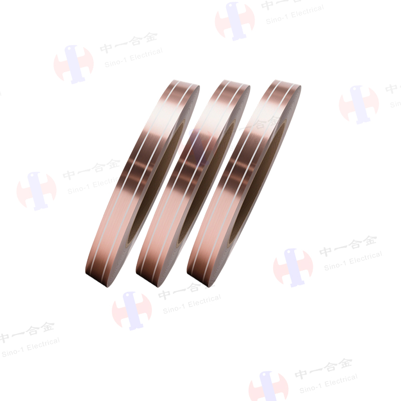
Versatile Formats: Strip configurations—including inlay, onlay, and overlay—allow engineers to customize the metal profile to match exact terminal, switch, or connector designs.
Manufacturing Readiness: Clad materials are highly compatible with high-speed progressive die stamping, though scrap recovery requires specialized handling.
Engineers face a persistent challenge when selecting materials for electrical contacts. You must carefully balance current-carrying capacity against structural longevity. Pure copper provides exceptional thermal and electrical pathways. It boasts a 100% International Annealed Copper Standard (IACS) rating. However, solid copper fails to sustain tension over time. It lacks the necessary spring characteristics. Repetitive mechanical stress in switches quickly leads to contact relaxation. You ultimately risk internal arcing and premature component failure.
Pure brass introduces a completely different set of challenges. Brass offers excellent machinability and durability. It resists environmental corrosion incredibly well. Yet, its electrical conductivity remains significantly lower. Brass typically hovers around 28% IACS. Sending high currents through solid brass generates unacceptable thermal rise. Overheating compromises surrounding plastics and dielectric insulators. Thermal expansion eventually degrades the entire terminal housing.
By bonding these metals at the atomic level, we create a specialized composite. The clad solution lets designers decouple electrical requirements from structural demands. You get the ideal material combination. The copper sector handles the heavy electrical load seamlessly. The brass base provides the necessary spring force and rigidity. This synergy effectively prevents common points of failure in complex electrical assemblies.
The physical arrangement of clad layers directly dictates component performance. Engineers can specify highly precise cross-sectional geometries. This customization maximizes material savings and operational efficiency. Let us examine the three primary configurations used extensively in modern electrical designs.
Mechanism: Copper is embedded flush into a brass base.
Best For: Flush electrical contacts, sliding switches, and components where strict dimensional tolerances are required across the strip's width.
An inlay clad metal strip keeps the material surface entirely uniform. You rely on this format when the mating component needs a smooth sliding path. It eliminates mechanical bumps while providing a localized high-conductivity zone. The surrounding brass handles the friction forces.
Mechanism: Copper is bonded to the surface of the brass but raised above the base material.
Best For: Raised contact points, breaker terminals, and applications requiring a defined physical separation or mechanical wiping action.
An onlay clad metal strip acts as an integrated contact rivet. The elevated copper strip ensures the electrical connection occurs exactly at the highest point. You achieve reliable circuit closure while minimizing expensive copper usage. This raised profile also helps clear microscopic debris during contact mating.
Mechanism: Continuous layers of copper and brass bonded across the entire width (single-sided or double-sided).
Best For: Busbars, lead frames, and heavy-duty current carriers where uniform surface conductivity is required over a stronger structural core.
An overlay clad metal strip acts as a robust bimetal sheet. It easily handles massive current distribution networks. The continuous copper layer mitigates surface-level resistance entirely. Meanwhile, the thicker brass core prevents the busbar from warping under intense physical stress.
Configuration Type | Surface Profile | Primary Advantage | Ideal Application |
|---|---|---|---|
Inlay | Flush and uniform | Zero mechanical interference | Sliding contacts |
Onlay | Raised copper ridge | Concentrated contact pressure | Microswitches |
Overlay | Fully coated width | Maximum surface conductivity | Power busbars |
When integrating these composites, we must rigorously assess their behavior under real-world conditions. A thorough evaluation ensures long-term field reliability. Let us break down the core performance dimensions into three distinct areas.
Electrical & Thermal Management: Heat dissipation pathways remain highly localized to the copper layer. This prevents thermal degradation of the brass spring base during continuous current loads. High currents always generate localized heat at the mating point. The copper pulls this dangerous heat away swiftly. Consequently, the structural brass retains its temper and original spring force over decades of continuous use.
Formability and Machining: Assessing the transition from raw strip to finished clad metal stamping parts reveals excellent overall ductility. The composite material handles complex bends effortlessly. You can execute deep drawing processes without risking delamination. The atomic bond stretches uniformly during high-speed progressive stamping operations. Engineers rarely need to slow down press speeds.
Wear Resistance and Cycle Life: The brass substrate provides superior fatigue resistance. Components subjected to high insertion and extraction cycles absolutely demand this resilience. EV charging pins and relay springs rely heavily on this dual-nature performance. They maintain strong contact pressure through thousands of mating cycles. The copper surface conducts power, while the brass resists mechanical wear.
Transitioning to clad materials introduces specific manufacturing challenges. We must transparently assess these risks to avoid unexpected production delays. Ignoring these realities often leads to compromised final assemblies.
Layer separation is extremely rare in high-quality roll-bonded materials. However, improper bend radii during the stamping process can severely stress the clad interface. Sharp bends might exceed the structural elongation limits of the outer layer. Vendor testing remains absolutely mandatory. You should request comprehensive bend tests and thermal shock tests before approving any new material batch. Always verify the bond integrity under physical duress.
Stamping solid metals yields easily recyclable scrap. Single-alloy scrap commands high market returns. Conversely, scrap from composite stamping is a mixed-metal alloy. This mixed scrap predictably carries a lower salvage value. Metallurgical separation processes are complex and highly energy-intensive. You must factor this lower recovery rate into your financial planning and scrap management strategy. Do not assume parity with solid copper scrap pricing.
Post-stamping operations shear the metal. The edges of the finished component will expose both base metals simultaneously. This bimetallic junction can become problematic. In highly corrosive environments, moisture can easily trigger galvanic localized corrosion. Protective plating may still be strictly required. Tin or nickel flashing effectively seals these exposed edges against environmental degradation. We recommend edge plating for marine or automotive applications.
Failing to specify generous bend radii in the initial tooling design.
Assuming composite scrap yields the same financial return as solid pure metal scrap.
Deploying bare-edged stamped parts in high-humidity industrial environments.
Selecting the right material partner ensures strict product consistency. You need a vendor capable of exacting metallurgical control. Consider the following specification logic when evaluating potential suppliers.
Specify the exact thickness ratio based on the minimum cross-sectional area required. For instance, you might request 10% Copper and 90% Brass. This ratio must adequately support the peak continuous current load. Over-specifying the copper layer severely erodes the material's cost benefit. You should calculate the lowest safe copper volume needed for adequate thermal management. Rely on parallel circuit calculations to determine the exact cross-section.
The cladding and annealing processes fundamentally alter the grain structure of both metals. Ensure your supplier can provide the required temper accurately. You might need half-hard or spring-hard properties for your connectors. The final temper must be guaranteed explicitly after all roll-bonding steps are complete. This guarantees the structural integrity of the final stamping. A mismatched temper leads to immediate spring failure.
Demand strict quality documentation during the crucial prototyping phase. Require cross-sectional micrograph reports from vendors. These high-resolution images visually verify the absence of microscopic voids. They confirm no oxides exist at the critical metallurgical bond line. You must validate this atomic bonding thoroughly before moving into full-scale production. Skipped validations frequently cause late-stage assembly rejections.
Specification Parameter | Engineering Goal | Validation Method |
|---|---|---|
Layer Ratio (e.g., 10/90) | Optimize conductivity vs. cost | Cross-sectional area calculation |
Final Material Temper | Ensure reliable spring properties | Tensile testing post-annealing |
Bond Line Integrity | Prevent stamping delamination | Micrograph report analysis |
Provide your vendor with detailed CAD models of the intended stamping process.
Request lot-to-lot consistency guarantees in the purchasing agreement.
Review the vendor's internal ultrasonic testing capabilities for defect detection.
Brass-copper clad metals are not just a cost-reduction exercise. They serve as a highly targeted engineering solution for high-performance electrical components. By utilizing inlay, onlay, or overlay techniques, manufacturers can engineer the exact balance of conductivity and strength. You effectively eliminate the traditional compromises found in single-alloy designs. The atomic bond delivers power efficiently while maintaining structural dominance.
Engineers evaluating this transition should calculate their required current-carrying capacity precisely. You must determine the optimal clad ratio for your specific application. Next, request material samples for high-speed stamping trials. These trials validate tool wear and confirm structural performance in your own facility. Proactive testing ensures a perfectly smooth transition to these superior composite materials.
A: Yes. The copper surface retains its inherent solderability and weldability. This makes it ideal for wire attachments and terminal joining. Meanwhile, the brass base can be used securely for mechanical fastening. You get optimal joining properties on both sides of the composite material.
A: While capabilities vary by manufacturer, typical inlay thicknesses can be engineered down to a few microns. Extreme thinness may limit high-current applications. You should always align the inlay depth with your specific thermal and electrical load requirements.
A: It is calculated using the parallel circuit rule based on the cross-sectional area of each metal. It will be lower than pure copper but exponentially higher than pure brass. The final conductivity is tailored specifically to your defined material ratio.
A: Generally, no. Progressive dies used for brass or copper can process clad metals. However, die clearance and bend radii must be optimized. This accommodates the combined mechanical properties and prevents sheer stress on the metallurgical bond line.